
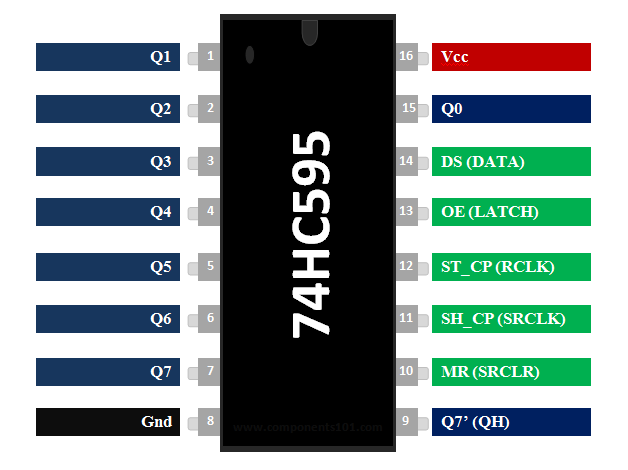
| Pin Number | Pin Name | Description |
| 1,2,3,4,5,6,7 | Output Pins (Q1 to Q7) | The 74hc595 has 8 output pins out of which 7 are these pins. They can be controlled serially |
| 8 | Ground | Connected to the Ground of the circuit |
| 9 | (Q7) Serial Output | This pin is used to connect more than one 74hc595 as cascading |
| 10 | (MR) Master Reset | Resets all outputs as low. Must be held high for normal operation |
| 11 | (SH_CP) Clock | This is the clock pin to which the clock signal has to be provided from MCU/MPU |
| 12 | (ST_CP) Latch | The Latch pin is used to update the data to the output pins. It is active high |
| 13 | (OE) Output Enable | The Output Enable is used to turn off the outputs. Must be held low for normal operation |
| 14 | (DS) Serial Data | This is the pin to which data is sent, based on which the 8 outputs are controlled |
| 15 | (Q0) Output | The first output pin. |
| 16 | VCC | This pin powers the IC, typically +5V is used |
Features
- 8-bit, Serial In – Parallel out Shift register
- Operating Voltage: 2V to 6V
- Power Consumption: 80uA
- Output source/sink current: 35mA
- Output Voltage is equal to Operating voltage
- Minimum high-level Input Voltage: 3.15V @(Vcc=4.5V)
- Maximum low-level Input Voltage: 1.35V @(Vcc=4.5V)
- Can be easily cascaded with more IC to get more outputs
- Maximum Clock Frequency: 25Mhz @4.5V
- Available in 16-pin PDIP, GDIP, PDSO packages
Link zu einer Experimentier-Seite: http://moba.noethlich.info/?page_id=297